Most Popular
-
1
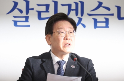
First-ever meeting of president, opposition chief set to finally happen
-
2
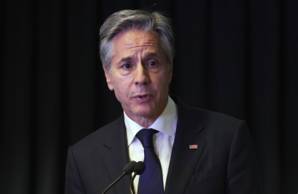
Blinken calls on China to press N. Korea to end its 'dangerous' behavior
-
3
Naver’s Line ownership in jeopardy as Japan ups pressure

-
4
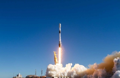
South Korea to launch space security center under spy agency
-
5
More med professors to take day off each week while govt. urges them to stay


-
6
Hybe refutes Ador CEO Min's denial of breach of trust
-
7
S. Korea, Japan could consider simplified entry agreement: Seoul official
-
8
[Weekender] How DDP emerged as an icon of Seoul
![[Weekender] How DDP emerged as an icon of Seoul](//res.heraldm.com/phpwas/restmb_idxmake.php?idx=644&simg=/content/image/2024/04/25/20240425050915_0.jpg&u=)
-
9
New celebrity-endorsed therapy for face contouring requires only a pair of rubber bands
-
10
[Today’s K-pop] NewJeans' single teasers release amid intrigue
![[Today’s K-pop] NewJeans' single teasers release amid intrigue](//res.heraldm.com/phpwas/restmb_idxmake.php?idx=644&simg=/content/image/2024/04/26/20240426050575_0.jpg&u=)


![[Weekender] How DDP emerged as an icon of Seoul](http://res.heraldm.com/phpwas/restmb_idxmake.php?idx=644&simg=/content/image/2024/04/25/20240425050915_0.jpg&u=)

![[Today’s K-pop] NewJeans' single teasers release amid intrigue](http://res.heraldm.com/phpwas/restmb_idxmake.php?idx=644&simg=/content/image/2024/04/26/20240426050575_0.jpg&u=)

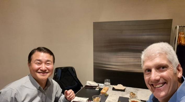
Samsung chief returns from Netherlands, satisfied with ASML deal
Deal with ASML raises possibility that Samsung could get ahead in producing cutting-edge 2-nanometer chips
By Jo He-rimPublished : Dec. 15, 2023 - 15:10
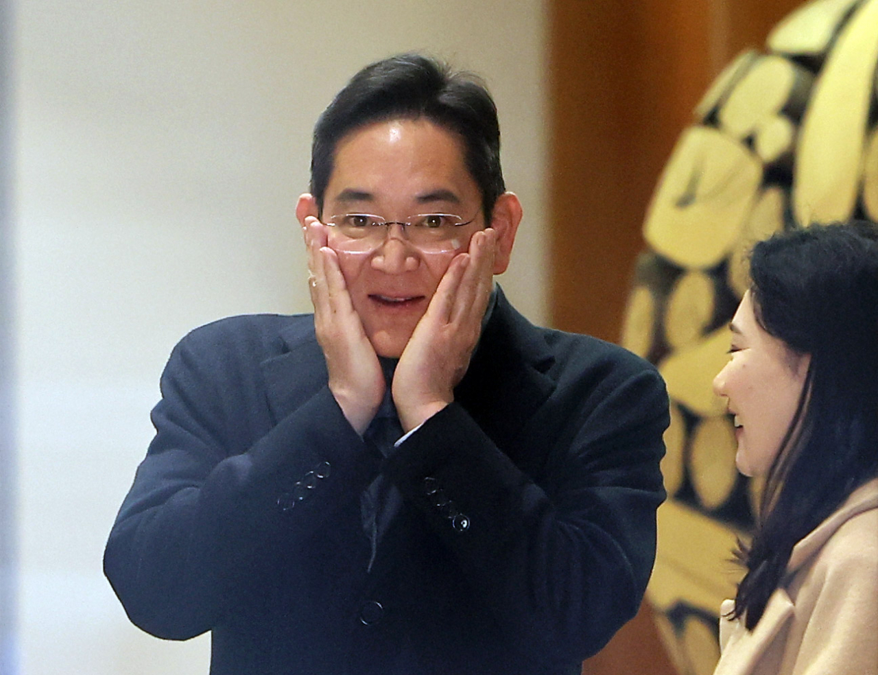
Samsung Electronics Chairman Lee Jae-yong hinted at his satisfaction over his trip to the Netherlands with President Yoon Suk Yeol on Friday, saying that most of the achievements made there were focused on semiconductors.
"About 90 percent of the achievements made in the trip to the Netherlands are on semiconductors,” Lee told reporters when asked about the achievements of the trip, at Gimpo International Airport on Friday, with a satisfied smile on his face.
Lee returned from the trip to the European country in the early morning. He had accompanied the president during the four-day state visit to meet with Dutch leaders as well as the heads of prominent Dutch chip equipment firms, including ASML, to forge a number of deals.
ASML is the sole manufacturer of EUV equipment -- a key system for producing the world's most advanced semiconductor chips with nodes at 7 nanometers and below -- with unrivaled technology.
Securing an order of the ASML's EUV machines, of which only 40 to 50 units per year are produced, has become a mission for global chip suppliers, as the equipment is deemed a crucial factor that can sway chipmakers' survival in the market.
Samsung, the world's top memory chipmaker by revenue, inked a 1-trillion-won ($762 million) deal with the Dutch equipment supplier to build a research facility for developing highly advanced EUV technology in Korea.
Samsung Electronics Vice Chairman Kyung Kye-hyun, head of the Device Solutions Division, which oversees the company’s chip business, also underscored that the latest agreements will support Samsung's priority to secure the Dutch firm's next-generation high-numerical aperture EUV lithography scanner equipment.
"Samsung has secured a priority over the High-NA equipment technology," Kyung said, as he arrived in the airport with Lee.
"(From the trip), I believe we created an opportunity for us to optimize the usage of High-NA technology for our production of DRAM memory chips and logic chips, in the long term," he said.
According to Kyung, Samsung and ASML will build a joint research facility in Dongtan, Gyeonggi Province and bring the High-NA EUV equipment into the facility. There, the engineers of the two companies will work together to enhance the chipmaking process, Kyung said.
"Rather than focusing on how fast we bring the High-NA EUV machine into Korea, it is more important for us to build the partnership (with ASML) so that Samsung can better use the next-generation equipment," Kyung said, adding that Samsung did forge a strong partnership with a very "sturdy ally."
The high-NA EUV equipment raises the lens' numerical aperture -- indicating its light-collecting ability -- from 0.33 to 0.55, allowing chip manufacturers to utilize ultrafine patterning technology to produce 2nm-node chips.
ASML is preparing to launch the product for the first time in the industry in the coming months.
ASML is expected to supply 10 units of the High-NA EUV equipment to the market next year, and Intel has reportedly secured six of them. The Dutch firm said it aims to increase annual production of the new product to 20 in the coming years.
With the goal to catch up to market leader TSMC in the foundry business, Samsung's foundry division announced it will start production of chips with 2nm nodes in late 2025.